")


來自美國的SVTA自1993便投身於超高真空分子束磊晶與各式薄膜沈積技術,並創建前瞻材料實驗室積極與NASA等知名機構合作、厚植技術實力,這讓SVTA成為半導體技術研發的領航者。
SVTA針對不同材料之磊晶,提供一系列MBE系統供用戶選擇:氮化物MBE系統、氧化物MBE系統、III-V II-VI MBE系統、矽MBE系統;此外SVTA也提供多種高品質配件與可擴充項目供用戶選擇,增加使用MBE的彈性。SVTA MBE分子束磊晶系統的產品特色如下:
- 超高真空作業環境,完全杜絕基材在磊晶過程被污染的疑慮
- 可依照需求,將MBE系統配置為線型(in-line)或是枚葉型(cluster)之形式
- 可依材料特性(wetting、clogging等),選擇恰當的Effusion Cell蒸發源
- 眾多可擴充項目:電漿源、氣體注射器等
Fully Automated Cluster MBE System
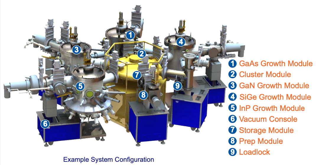
Automated System Controls:
- Programmable fully automatic recipes ensure run-to-run process repeatability
- Integrated real-time display of processing variables together onto one screen
- Logging of parameters including wafer number and history exportable to Microsoft Excel
Safety Features:
- Automated wafer handler for safe operation
- Control software with adjustable access limits
- Emergency Off(EMO) Switch
- Individual Vacuum and Chamber Interlocks for independent Operation and Cross Contamination Control
Optional Features:
- MBE Growth Modules
- Glove Box Integration
- UHV ALD Deposition Modules
- STM/AFM and XPS Modules
Technical Specifications:
- Console: Cleanroom Compatible
- Footprint: 500cmx500cm
- Process Modules: Up to 7
- Platen Size: Up to 6.0 Sample Size
- Base Pressure: <1.0x10 -10 Torr
- Transfer Speed: < 5 Minutes (Buffer to Modules)
- Control Computer: Desktop PC
- Control Software: ROBO MBE Cluster Tool Software with independent ROBO MBE Growth Software
R&D-Oriented High Performance MBE Systems
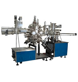
III-V II-VI MBE系統
本系統專用於成長高質量的化合物半導體材料,可製備具有高載流子遷移率和低缺陷的化合物半導體材料。III-V和II-VI MBE系統可使用SVTA的裂解器蒸發源(cracking sources),針對固體和氣體材料進行磊晶作業。系統基本規格如下:
- 基材尺寸:4”晶圓x1片
- 基材加熱:最高至1,000˚C
- 蒸發源埠口:10組
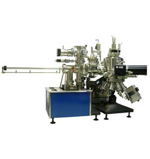
Nitride MBE系統
本系統是專門用於生長高質量的氮化鎵、氮化鋁及氮化物材料,長晶腔體透過配置RF電漿源或氨氣(Ammonia)注入器來處理活性氮含量問題,此外配備高溫襯底加熱器可以使薄膜成長更為均勻。系統基本規格如下:
- 基材尺寸:3~8”晶圓x1片
- 基材加熱:標準1000˚C,選配可達1200˚C
- 蒸發源埠口:7~8組

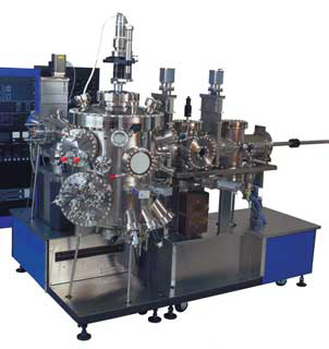
Oxide MBE系統
本系統專門用於成長高質量的超導膜和金屬氧化物半導體材料。長晶模組經特殊設計可在高活性氧的環境中運作,另外模組內配置具備抗氧設計的基板加熱器,製程所需的氧氣由RF電漿源或臭氧(Ozoe,O3)輸送源產生。系統基本規格如下:
- 基材尺寸:3~8”晶圓x1片
- 基材加熱:標準1,000˚C,選配可達1,200˚C
- 蒸發源埠口:8~10組
Silicon MBE系統
本系統專為滿足成長 IV-IV 材料和相關矽半導體化合物而設計,配備有電子束蒸發源及電子感應器反饋機制,可以確保高品質的矽磊晶具備再現性。系統基本規格如下:
- 基材尺寸:4”晶圓x1片
- 基材加熱:最高至1,000˚C
- 蒸發源埠口:10組